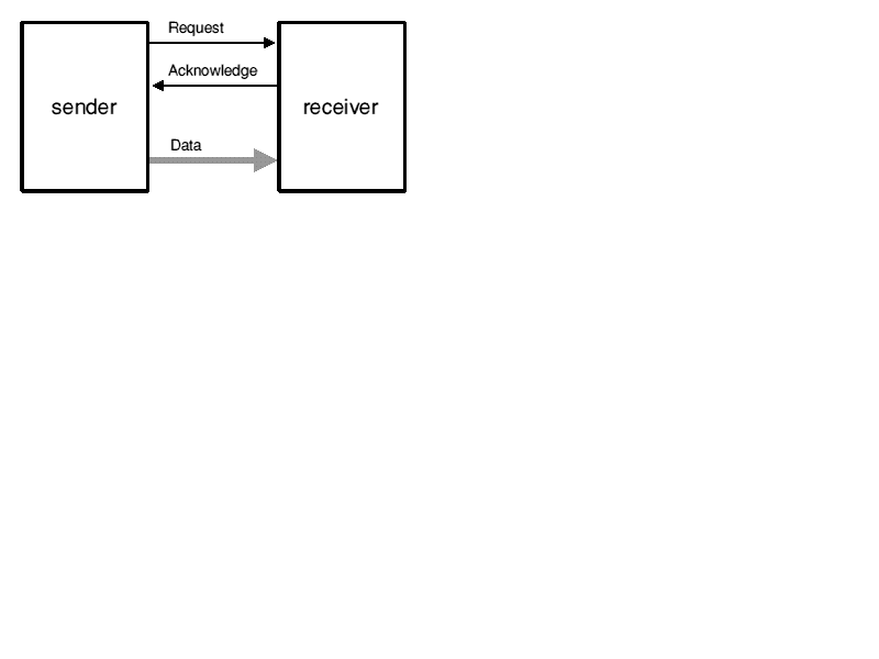
Figure 1: The Bundled Data Interface Used in a Micropipeline
There is a world-wide resurgence of interest in asynchronous logic design techniques. After two decades during which clocked logic has imposed its discipline across all corners of the world of digital logic, the older and more anarchic approach seems poised to make a come-back.
Asynchronous design does not follow this methodology; in general there is no clock to govern the timing of state changes. Subsystems exchange information at mutually negotiated times with no external timing regulation.
As synchronous techniques have improved, tools have been developed which automate most of the design processes. The design of a complete chip can now be synthesized from a high level behavioural description with minimal manual intervention. Synchronous design is at the top of the learning curve and seems set to continue its domination of digital systems for the forseeable future.
For some time now it has been difficult to sustain the synchronous framework from chip to chip at maximum clock rates. On-chip phase-locked loops help compensate for chip-to-chip tolerances, but above about 50MHz even this isn't enough.
Building the complete CPU on a single chip avoids inter-chip skew, as the highest clock rates are only used for processor-MMU-cache transactions. However, even on a single chip, clock skew is becoming a problem. High-performance processors must dedicate increasing proportions of their silicon area to the clock drivers to achieve acceptable skew, and clearly there is a limit to how much further this proportion can increase. Electrical signals travel on chips at a fraction of the speed of light; as the tracks get thinner, the chips get bigger and the clocks get faster, the skew problem gets worse. Perhaps the clock could be injected optically to avoid the wire delays, but the signals which are issued as a result of the clock still have to propagate along wires in time for the next pulse, so a similar problem remains.
Even more urgent than the physical limitation of clock distribution is the problem of heat. CMOS is a good technology for low power as gates only dissipate energy when they are switching. Normally this should correspond to the gate doing useful work, but unfortunately in a synchronous circuit this is not always the case. Many gates switch because they are connected to the clock, not because they have new inputs to process. The biggest gate of all is the clock driver, and it must switch all the time to provide the timing reference even if only a small part of the chip has anything useful to do. Often it will switch when none of the chip has anything to do, because stopping and starting a high-speed clock is not easy.
Early CMOS devices were very low power, but as process rules have shrunk CMOS has become faster and denser, and today's high-performance CMOS processors can dissipate 20 or 30 watts. Furthermore there is evidence that the trend towards higher power will continue. Process rules have at least another order of magnitude to shrink, leading directly to two orders of magnitude increase in dissipation for a maximum performance chip. (The power for a given function and performance is reduced by process shrinking, but the smaller capacitances allow the clock rate to increase. A typical function therefore delivers more performance at the same power. However you can get more functions onto a single chip, so the total chip power goes up.) Whilst a reduction in the power supply voltage helps reduce the dissipation (by a factor of 3 for 3 Volt operation and a factor of 6 for 2 Volt operation, relative to a 5 Volt norm in both cases), the end result is still a chip with an increasing thermal problem. Processors which dissipate several hundred watts are clearly no use in battery powered equipment, and even on the desktop they impose difficulties because they require water cooling or similar costly heat-removal technology.
As feature sizes reduce and chips encompass more functionality it is likely that the average proportion of the chip which is doing something useful at any time will shrink. Therefore the global clock is becoming increasingly inefficient.
What has happened to all the problems that caused the world to go synchronous in the first place? These have not just ceased to exist, but they have become less overwhelming for the designer. Over the years the academics have improved the methodologies which can be applied to the design of asynchronous circuits, so a lot more is known about the reliability and correctness of potential solutions. But perhaps most important is the increasing capability of VLSI technology. This enables ready-made solutions to standard problems to be prepackaged in a design library, removing the need for each designer to understand fully all the intricacies of asynchronous design. There are now so many transistors on a chip that the inefficiency of using a standard asynchronous solution is negligible compared with the extra design cost of customising each occurrence.
The most popular form in recent years has been dual-rail encoding with level sensitive signalling. Full delay insensitivity is still achieved, but there must be a "return to zero" phase in each transaction, and therefore more power is dissipated than with transition signalling. The advantage of this approach over transition signalling is that the logic processing elements can be much simpler; familiar logic gates process levels whereas the circuits required to process transitions require state and are generally more complex. The Tangram compiler developed at Philips Research Laboratories in the Netherlands uses this style to transform high-level function specifications written in an Occam-like language into silicon layout, a technique named "VLSI programming" by its inventors [1].
In 1987, Ivan Sutherland chose the topic of asynchronous design for his Turing Award lecture. He presented an approach developed by Sutherland, Sproull and Associates called "Micropipelines" [2]. This approach uses bundled data with a transition signalled handshake protocol to control data transfers. This is illustrated in figures 1 and 2. Figure 1 shows the interface between the sender and receiver. There is a bundle of data which carries information (using one wire for each bit) and two control wires: Request from the sender to the receiver carries a transition when the data is valid; Acknowledge from the receiver to the sender carries a transition when the data has been used. The protocol sequence is illustrated in figure 2. This defines only the sequence in which events must occur - there is no upper bound on the delays between consecutive events.
Figure 1: The Bundled Data Interface Used in a Micropipeline
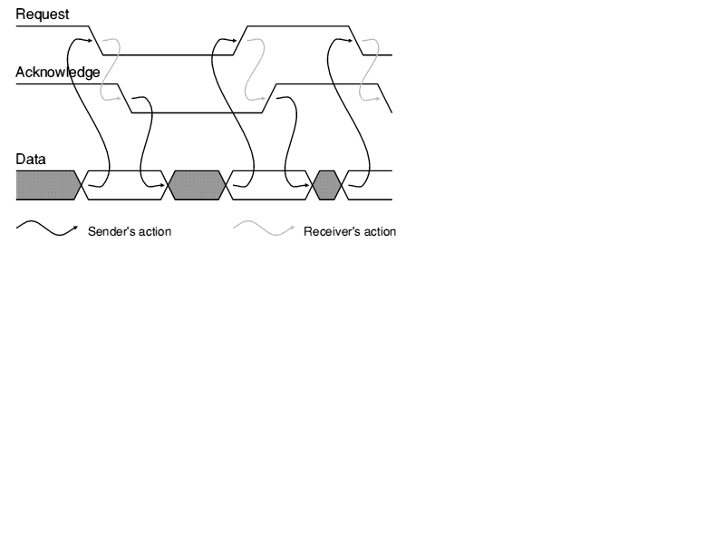
Figure 2: The Bundled Data Interface Protocol
Once the data bundling constraints are met (ie the order of events corresponds to that shown in figure 2), a micropipeline is delay-insensitive. The event processing blocks which are required to control the operation of all but the simplest micropipelines are well defined and relatively straightforward to design using existing asynchronous design techniques. Once designed, these blocks can be placed in a library and reused to construct arbitrarily complex control structures. No sophisticated design techniques are required to put these circuits together; conventional behavioural simulation is a useful aid, as is a large whiteboard. The only uniquely asynchronous problem which recurrs is the high-level issue of liveness (absence of deadlock).
The AMULET project at Manchester University adopted the micropipeline approach for the work described below.
Although a complete asynchronous microprocessor has been built before [3], this is the first attempt at a full-functionality design including the difficult area of exact exceptions for memory faults. New solutions were required for several areas of the design, for instance a novel register locking technique was developed to manage dependencies between the registers used by successive instructions [4]. The ALU exploits data dependent timing to deliver significantly faster operation for typical operands than for worst-case values [5]. The processor allows a considerable level of internal concurrency, with all the pipeline stages operating autonomously and only interacting with nearest neighbours when results are ready to be passed on. One result of the autonomy is that the depth of instruction prefetching beyond a branch is fundamentally non-deterministic (though it is bounded, and the instructions which are allowed to execute are deterministically defined!).
The initial phase of this work is now drawing to a close. The asynchronous ARM design is complete, and was submitted to fabrication in February 1993. Although the final verdict must await inspection of the silicon, it is already clear that this scale of design is now quite practical with existing design tools. The design resource required to complete the design was comparable with the clocked part, and although the transistor count and die area are rather larger than the synchronous version, most of the difference may be accounted to the deeper pipeline of the asynchronous design. A synchronous implementation which used the same pipeline structure would require perhaps 10 or 20% less area.
Asynchronous logic can be expected to begin winning niches in the digital electronics business within the next few years. It will share circuit boards with clocked chips and integrated circuits with clocked subcircuits. It will become established as a viable alternative technology in many areas, and the technology of choice for some.