The previous chapter has studied the organisation of superscalar pipelined synchronous processors. This chapter considers if and how this type of processor can be implemented using asynchronous logic. The first section explains the motivation for using asynchronous logic in low power systems. Subsequent sections consider the implementation of pipelines and superscalar parallelism using asynchronous logic, and considers ways in which instruction set features can make implementation simpler. The final section reviews previous asynchronous processors.
The SCALP processor uses asynchronous logic because this approach is believed to have benefits in terms of power efficiency and other factors. This section explains these benefits.
All systems, both synchronous and asynchronous, can be divided into regions of combinational logic separated by storage. In the two cases the speed of the combinational logic and of the storage elements will be approximately equal. The claim for increased performance for asynchronous systems comes from the observation that in synchronous systems the speed of the global clock must match the speed of the slowest logic block with its slowest input data. The consequence is that faster blocks will be idle for part of the clock cycle.
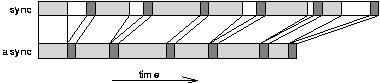
This is illustrated in the upper part of figure 4.1. The light areas represent processing delays in logic blocks; the dark areas represent storage delays. The cycle time of the global clock signal is set according to the slowest logic block. For the other blocks there is an idle period shown in white.
In an asynchronous system there is no global clock; local request and acknowledge signals indicate when a result is ready and it may advance immediately. This is shown in the lower part of figure 4.1; there are no idle periods between cycles. Consequently the overall speed of the system is increased[FOOTNOTE].
[FOOTNOTE] Asynchronous pipelines are subject to problems of starvation and blocking which can cause blocks to be idle at some points. This proviso is discussed in section 4.2.
This increase is especially significant when the speed of the logic is data dependent; the clock speed in a synchronous system would have to allow for the worst case data which may be very rare.
If asynchronous circuits can be faster than equivalent synchronous circuits then a power saving can be achieved; by adjusting the supply voltage the circuits can be made to operate at the same speed, but because of the reduced supply voltage the asynchronous circuit will do so using less power.
In some circumstances asynchronous circuits may be smaller than equivalent synchronous circuits. By reducing the size of the circuit a power saving can be made as fewer wires of smaller capacitance must be charged and discharged for each operation.
This type of advantage is best demonstrated by two datapath elements, adders and multipliers. In the case of an adder the main design problem is dealing with the carry signals. With a simple ripple carry design in the worst case the carry has to propagate across the whole width of the adder, though in typical cases it only needs to propagate for a few bits. In an asynchronous system this typical case delay is the important measure and the relatively small ripple carry adder is satisfactory. In a synchronous environment on the other hand it is the worst case delay that is important, and adder designs such as carry select adders are used. These designs provide better performance in the rare worst case but at a significant cost in terms of area. [GARS93] compares the ALUs from the synchronous ARM6 processor and the asynchronous AMULET1 processor. The ARM6 carry select adder is 2.5 times larger but operates at about the same speed for typical operands.
Asynchronous multipliers can be smaller than synchronous multipliers for a different reason. Multiplication using carry save adders is an example of an algorithm that performs a simple step a number of times in order to compute its result. In an asynchronous multiplier the simple carry save adder logic is exercised as many times as is necessary at high speed by local request and acknowledge signals. In a synchronous design on the other hand the global clock speed is typically limited by some other part of the design, and is many times slower than the carry save adders. In order to maintain a reasonable speed the synchronous designer makes a number of copies of the adders so that several stages of the computation can take place within one cycle. The result is a circuit that is no faster than the asynchronous design but is much larger. The increased size means that wires both within the multiplier and outside it will be longer and hence consume more power when they transition.
These examples of the area benefit of asynchronous logic must be balanced against any change in the the complexity and size of asynchronous control structures compared with equivalent synchronous circuits.
Perhaps the strongest case for the power efficiency benefit of asynchronous logic comes from the study of systems with variable processing demand. This sort of system is very common; most computers that operate interactively experience considerable and rapid fluctuations in processing demand as the user performs different tasks. In embedded applications it is also common; processors are activated in response to particular events, operate for a short time and are then suspended.
Synchronous processors take a coarse-grained approach to power saving in this situation. Portable computers for example monitor user activity and enter various types of sleep mode by slowing or stopping clocks as activity slows. They use this coarse-grained approach because switching between clocks is a complex procedure, and typically some interaction with the system software is needed.
In asynchronous systems the behaviour is quite different. In the absence of demand for processing, none of the request or acknowledge signals will be asserted. Consequently there is no circuit activity and no power is consumed. This provides an instantaneous response to changes in the computational demand and consequently a greater power saving than can be obtained with a synchronous system.
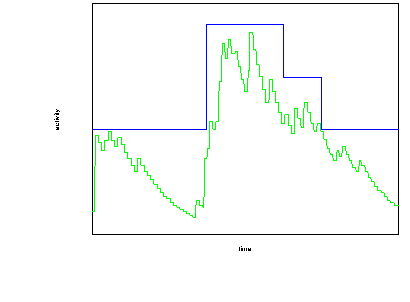
Figure 4.2 illustrates this. The lower line indicates processor activity. In an asynchronous implementation power consumption would be proportional to this activity level. In a synchronous implementation the clock speed would be adjusted more coarsely as shown by the upper line and the power consumption would be greater. The area between the two lines represents the power saving that the asynchronous processor would obtain.
Greater power savings can be obtained in a variable demand system if the system supply voltage is reduced when activity is low. In synchronous systems as with clock speed adjustment this approach can again only be applied at a coarse level, and the designer has to ensure that the clock rate and the supply voltage maintain a safe relationship. In an asynchronous system on the other hand feedback techniques can be used to continuously maintain the supply voltage at the minimum necessary level.
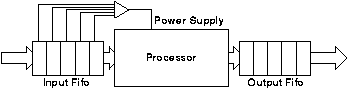
One possible scheme for digital signal processing applications is described in [NIEL94] and is shown here in figure 4.3. In this example incoming data is placed into a fifo. The occupancy of the fifo is measured and is used to set the supply voltage; as the fifo fills the supply voltage is increased so the processor operates faster, emptying the fifo.
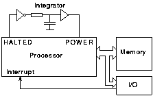
Another scheme suitable for a general purpose processor such as SCALP is shown in figure 4.4. This case relies on the program executing a HALT instruction when it has no useful work to do; in the case of SCALP, HALT means "wait for next interrupt". When the processor is halted it asserts an output. This output is integrated to derive an analogue level indicating the system load. This is used to adjust the supply voltage.
A common mode of operation for a synchronous circuit is as follows: in response to a clock edge, a number of signals change. As these changes propagate through the circuit outputs change possibly several times before reaching a stable value. These glitches do not cause the circuit to fail because the next piece of logic will not sample their value until the next clock edge; however every transition, useful or not, consumes power.
In an asynchronous circuit[FOOTNOTE] on the other hand every transition has a meaning. Any spurious transitions caused by hazards will cause the circuit to malfunction, so circuits must be designed to not create glitches. Consequently the asynchronous circuit may make fewer transitions and hence consume less power than an equivalent synchronous circuit.
[FOOTNOTE] This applies to many though not all classes of asynchronous circuits; see section 6.1. Specifically it applies to delay insensitive and speed independent circuits but may not apply to bounded delay circuits.
On the other hand it can be suggested that because these asynchronous circuits must be hazard free they will be more complex, which will in turn lead to greater power consumption. These two factors must be balanced for each particular application.
As well as the power efficiency issues discussed above there are other benefits of asynchronous logic that motivated its use in SCALP:
As an example of the potential power efficiency benefits of asynchronous logic, this section describes work carried out by Philips Research Laboratories using the VLSI Programming language Tangram. Tangram is an Occam-like high level language which is compiled into asynchronous circuits. The mathematical approach used makes formal reasoning about the circuits for purposes such as testability possible, and its high level nature allows designers to concentrate on architectural factors affecting the power efficiency.
Recent publications [KESS95] [BERK95] describe the implementation of an error detection circuit for a digital compact cassette (DCC) player. The nature of the application requires a constant data throughput, though the work required for each block of data is variable. The algorithm has two parts:
(i) error detection, which is applied to all input data,
(ii) generation of error correction information, which is only necessary when part (i) detects errors.
The solution used is as follows: the chip has two power inputs, one providing 1.5 V and the other 5 V. During part (i) the 1.5 V supply is used. During part (ii) if necessary the 5 V supply is used. In this way the system uses the lowest possible supply voltage. Interestingly no communication is required with the environment during part (ii), eliminating the need for voltage level shifters at the interface.
A synchronous implementation of the part already existed which uses a fixed 3 MHz clock which is gated to some parts of the chip when not needed and a fixed 5 V supply. In comparison the Tangram design is 20 % larger (due to the increased size of the control logic components) but gains a factor 5 power efficiency improvement through the use of asynchronous logic and a further factor of 20 through the use of dynamic supply voltage scaling.
Though the DCC chip is not a general purpose processor the techniques that it uses could be applied to one, with substantial power efficiency benefitis.
This section has presented a number of arguments suggesting that the use of asynchronous logic can provide power efficiency improvements, and mentioned a recent real design that seems to justify them.
For the SCALP design, the use of asynchronous logic is more important than just an implementation technology. Because SCALP is an entirely new design, the use of asynchronous logic can be taken into consideration throughout the design process including in the design of the instruction set. This issue is considered further in the following sections.
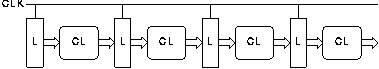
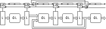
Figure 4.5 shows the familiar structure of a synchronous pipeline with latches (L) and combinational logic blocks (CL). All latches are controlled by a single global clock signal and so operate simultaneously.
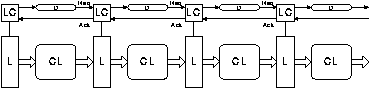
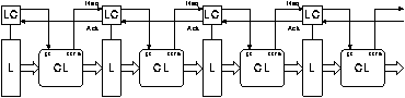
This form of pipeline is readily implemented asynchronously as shown in figures 4.6 and 4.7. The latches (L) and combinational logic blocks (CL) are the same as in the synchronous pipeline but the timing is controlled quite differently. Each latch has an associated latch control circuit (LC). The latch control circuit opens and closes the latch in response to request (Req) signals from the previous stage and acknowledge (Ack) signals from the following stage.
The request signal from the latch control circuit must be delayed by an amount greater than the corresponding data delay in the combinational logic. This may be done either using a matched path delay element (D) as shown in figure 4.6 or by using some form of completion detection as shown in figure 4.7.
The performance advantage of the asynchronous pipeline was mentioned in section 4.1.1 and is summarised in table 4.1. Note however that table 4.1 gives only an upper bound on the possible performance of asynchronous pipelines; performance can be decreased by starvation and blocking [KEAR95]. A pipeline stage is said to be starved if it cannot start an operation because it is waiting for the result of the previous stage to be available. Similarly a stage is said to be blocked if it cannot transfer its result to the next stage because that stage is still processing the result of the previous operation. Starvation and blocking are less significant in pipelines with small variations among the possible stage delays.
The effect of starvation and blocking on performance can be reduced by introducing decoupling queues between the stages. When one stage has to perform a particularly slow operation the queue preceding it will fill, preventing the previous stage from blocking. At the same time the queue following it will empty preventing the following stage from starving.
The performance of an asynchronous pipeline may also be reduced by delays introduced by the latch control circuit.
				Latency			Throughput
				determined by:		determined by:

Synchronous pipeline		Slowest block,		Slowest block,
				worst data,		worst data,
				worst conditions	worst conditions

Asynchronous pipeline		Typical block,		Slowest block,
with matched delays		worst data,		worst data,
				typical conditions	typical conditions

Asynchronous pipeline		Typical block,		Slowest block,
with completion detection	typical data,		typical data,
				typical conditions	typical conditions
The simple linear pipelines described above benefit from asynchronous implementation. Unfortunately the presence of forwarding paths as described in section 3.5.2 in processor pipelines makes efficient asynchronous implementation more difficult.
In a synchronous pipeline forwarding is simple to implement as shown in figure 4.8. Stage 2 uses as input the results of stages 1 and 3. Because all stages use a single clock these inputs are available at the same time.
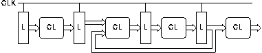
Figure 4.9 shows how this can be implemented asynchronously[FOOTNOTE]. The datapath is the same as in the synchronous pipeline; however the control is modified so that a request is sent to stage 2 when data from stages 1 and 3 are both available. A Muller C element[FOOTNOTE] is used to perform this synchronisation. Similarly the acknowledge signal from stage 2 is sent to both stages 1 and 3. Stage 3 waits for acknowledgements from stages 2 and 4 using a second Muller C element.
[FOOTNOTE] Some additional logic is required to ensure correct initialisation.
[FOOTNOTE] A Muller C element behaves as follows: when both inputs are high, the output becomes high. When both inputs are low, the output becomes low. When the inputs differ the output retains its previous level.
The additional timing constraints in this circuit make it adopt a form of locally synchronous behaviour, constraining the progress of instructions along the pipeline. This leads to a reduction in performance compared with the simple asynchronous pipeline.
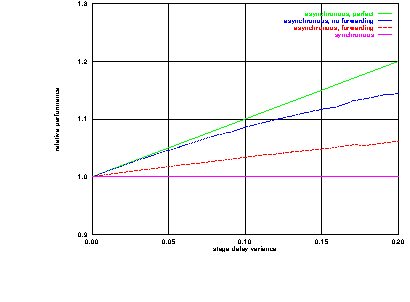
The extent of this performance reduction has been found for an example pipeline by simulation. The results are shown in figure 4.10. The figure shows performance for synchronous and asynchronous pipelines with and without forwarding. The pipeline concerned is a four stage pipeline with random stage delays of 1 [PLUSMINUS] v time units where v is the variance shown on the x axis. The y axis shows performance relative to the synchronous implementation.
The top line shows the performance of a perfect asynchronous pipeline. This perfect performance is not achieved because of starvation and blocking within the pipeline. The second line indicates the performance of a pipeline allowing for starvation and blocking. The third line indicates the performance of a pipeline with an unconditional forwarding path between the third and second stages.
When the variance is 0.2 (for example stage delays are equiprobably 0.8 and 1.2 time units) the perfect asynchronous pipeline's throughput is 20 % higher than the synchronous pipeline. Allowing for starvation and blocking this advantage is reduced to 14 %. When the forwarding path is introduced it is further reduced to only 6 %.
Operands provided via forwarding paths are not always used by the stages to which they are sent. Typically the receiving stage uses a multiplexor to select between the forwarded value and a value received from the previous stage. This multiplexor is controlled by a bit generated during instruction decode that indicates whether forwarding should be used (see figures 3.8 and 3.9).
In principle this conditional nature of forwarding could be used to improve the performance of asynchronous forwarding pipelines. When forwarding is not to be used no additional synchronisation is carried out and performance is similar to that of a simple asynchronous pipeline. When forwarding is required temporary additional synchronisation can be introduced to allow the forwarded data to be transferred.
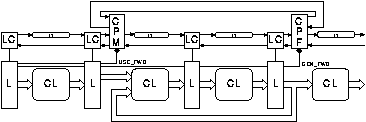
Such a scheme could be implemented as shown in figure 4.11: the instruction decode generates two bits for each instruction, one (USE_FWD) indicating that the instruction must use a forwarded value produced by a preceding instruction and another (GEN_FWD) indicating that the instruction must send its result to be used by a following instruction. At the pipeline stage where the forwarded data is used a "conditional pipeline merge" (CPM) element synchronises with forwarded data only when the USE_FWD bit is asserted. At the pipeline stage where the forwarded value is created a "conditional pipeline fork" (CPF) element sends the forwarded value only when the GEN_FWD bit is asserted.
The flaw with this proposal is that with conventional instruction sets it is impossible for the instruction decoder to generate the GEN_FWD bit. The USE_FWD bit can be generated as shown in figure 3.9, but to generate the GEN_FWD bit it would be necessary to know the operand registers of future instructions before they are issued.
One solution to this problem is to change the nature of the instruction set so that the need to forward a value can be detected by the instruction decoder. This may be done by giving more information about the way in which a result will be used in the instruction that produces that result. This technique is referred to here as "explicit forwarding".
One example of explicit forwarding is the scheme described in section 2.1.2 for using shorthand to transfer values between adjacent instructions without specifying register numbers.
Other systems can take the idea further. SCALP entirely replaces the conventional idea of accessing operands by means of register numbers with a system based on explicit forwarding. This is described further in chapter 5.
This section briefly considers the implementation and performance of general asynchronous superscalar structures in comparison with equivalent synchronous structures.
Figure 4.12 shows a synchronous parallel structure comprising an "issuer" (I) and a number of functional units (F1 to F3). Each of these blocks operates from the same global clock and so the performance of the system is limited by slowest block.
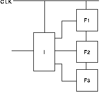
Figure 4.13 shows an equivalent asynchronous structure. In this case there is no global clock and performance is determined by the typical block speed. In fact the advantage of this structure over the synchronous circuit is greater than the advantage of an asynchronous pipeline over a synchronous pipeline. Even in an asynchronous pipeline throughput is limited by the slowest block. With this parallel arrangement this is not the case and throughput as well as latency is determined by the typical block speed. Furthermore for this parallel structure there is no equivalent of the starvation and blocking problem that affects asynchronous pipelines. This is summarised in table 4.2 which can be compared with table 4.1 for pipelines.
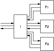
				Latency			Throughput
				determined by:		determined by:

Synchronous superscalar		Slowest block,		Slowest block,
processor			worst data,		worst data,
				worst conditions	worst conditions

Asynchronous superscalar	Typical block,		Typical block,
processor with matched delays	worst data,		worst data,
				typical conditions	typical conditions

Asynchronous superscalar	Typical block,		Typical block,
processor with completion	typical data,		typical data,
detection			typical conditions	typical conditions
The disadvantage of the asynchronous parallel implementation of figure 4.13 is that the issuer which distributes work to the various functional units must be more complex. In the synchronous implementation the issuer must make a decision about what to issue once per cycle; it studies the incoming instructions, looks at the state of the functional units and decides to issue one or two instructions. In the asynchronous implementation the task is more complex as the functional units can become ready to accept the next instruction at any time. Is is also possible that both units can become ready at the same time; in this case the issuer must arbitrate between them to decide which will receive the next instruction.
As in the single asynchronous pipeline forwarding makes implementation more difficult, but in this case forwarding is required both within and between the pipelines. To provide unconditional forwarding between all necessary points virtually every stage in every functional unit has to be synchronised with every other, leading to global lockstep behaviour and substantially reduced performance.
As for pipelines instruction set extensions may be used to make conditional forwarding and conditional synchronisation possible. This will lead to more independence between the pipelines and better performance.
The idea of explicit forwarding can be extended to superscalar processors; each functional unit output is connected by a conditional forwarding path to each functional unit input. Instructions explicitly indicate to where their results must be sent to so that only the necessary forwarding paths need be activated.
Unfortunately the non-deterministic allocation of instructions to functional units makes this form of explicit forwarding impossible. If an instruction's result is used by a particular following instruction then the first instruction must indicate that its result is sent to the functional unit that will execute the following instruction. That functional unit must therefore be known to the compiler.
This is not a problem when the functional units are asymmetric. If one functional unit executes loads and stores, another executes floating point instructions and another executes integer instructions, for example, then it is statically known which functional unit must execute each instruction, allowing explicit forwarding. When some instructions can be executed by more than one functional unit then the allocation must be known by the compiler. This can be achieved by performing the allocation of instructions to functional units in the compiler and encoding the appropriate functional unit identifier in the instruction.
This is essentially the system used by SCALP. Each instruction indicates the destination functional unit input to which its result should be sent. At the destination functional unit inputs forwarded data is paired with instructions arriving from the instruction issuer in much the same way that a reservation station matches instructions with data.
The SCALP architecture is described in the following chapter.
A number of asynchronous microprocessors have been proposed or built recently. This section describes the architecture and asynchronous design style of each[FOOTNOTE]. Table 4.3 summarises these characteristics.
[FOOTNOTE] The asynchronous design styles are defined in section 6.1.
Processor	Design Style	Instruction set	Organisation

CAP		4-phase,	Own 16-bit	Fetch-execute pipeline
		Dual rail,	RISC-like
		Delay
		insensitive

AMULET1		2-phase,	ARM		Pipelined,
		Bundled data			No forwarding

AMULET2		4-phase,	ARM		Pipelined,
		Bundled data			Forwarding

NSR		2-phase,	Own 16-bit	Pipelined,
		Bundled data	RISC-like	No forwarding,
						Decoupled load/store and branch

Fred		2-phase,	based on	Pipelined,
		Bundled data	88100		Multiple functional units,
						Single Issue,
						No forwarding,
						Decoupled load/store and branch

CFPP		2-phase,	SPARC		Pipelined,
		Bundled data			Multiple execution stages,
						Single Issue,
						Forwarding using counter-flow
						result pipeline

Hades		unspecified	Own		Pipelined,
						Multiple functional units,
						Multiple issue,
						Forwarding

ECSTAC		Fundamental	Own		Pipelined,
		mode		Variable length	No forwarding

TITAC		2-phase,	Own 8-bit	Non-pipelined
		Dual rail,
		Quasi delay
		insensitive

ST-RISC		Dual rail,	Own		Fetch-execute pipeline
		Delay
		insensitive

FAM		Dual rail,	Own RISC-like	Pipelined.
		Delay
		insensitive,
		4-phase

STRiP		Variable clock	MIPS-X		Pipelined,
		synchronous			Forwarding

SCALP		4-phase,	Own		Pipelined,
		Bundled data			Multiple functional units,
						Multiple Issue,
						Explicit forwarding
The first recent asynchronous processor was built by Alain Martin at Caltech [MART89]. The processor was described using a CSP-like notation which was compiled to a circuit description by means of program transformations. The resulting circuit is delay insensitive, using dual rail signalling.
The processor has a "RISC-like" load/store instruction set with 16 registers. It consists of a number of concurrent processes responsible for instruction fetch, operand read, ALU operate etc. The processor has been implemented in a 1.6 [MU]m CMOS process, and operates at 18 million instructions per second (MIPS) at room temperate and 5 V. The circuit continues to function at very low supply voltages, with optimum energy per operation at around 2 V. It has also been tested in liquid nitrogen at 77 K when its performance reaches 30 MIPS.
The AMULET group led by Steve Furber at the University of Manchester built AMULET1, the first asynchronous implementation of a commercially important instruction set [PAVE94]. AMULET2 is a similar processor still under development which also implements the ARM instruction set.
The ARM instruction set was designed for synchronous implementation [FURB89], and some of its features were included because they were convenient in the synchronous system. AMULET1 and AMULET2 implement this instruction set "warts and all", with some of these features leading to complexity and overheads. AMULET1 and AMULET2 implement the difficult areas of interrupts and exceptions.
AMULET1 was designed using a 2-phase bundled data design style based on [SUTH89]. It has a 5-stage execute pipeline (register read, multiply/shift, ALU, empty stage, register write) but does not provide for result forwarding. A locking mechanism is used to stall instructions at the register read stage until their operands have been written by previous instructions. Consequently the pipeline throughput is low.
Similar problems affect branch instructions. A branch instruction has to pass through 10 pipeline or fifo stages between being fetched and the target address being sent to memory. This results in large numbers of prefetched instructions being discarded and significant periods during which the pipeline is stalled.
AMULET1 permits out of order completion of load instructions relative to normal ALU instructions, though the instructions must commit to completing without fault in order.
Comparison of AMULET1 with the synchronous ARM processor is shown in table 4.4 (from [PAVE94]).
			AMULET1			ARM6

Process			1.2 [MU]m 2-layer metal	1.2 [MU]m 2-layer metal
			CMOS			CMOS

Cell core area		5.5 mm x 4.1 mm		4.1 mm x 2.7 mm

No. of transistors	58,374			33,494

Performance		9 K Dhrystones		14 K dhrystones @ 10 MHz

Dissipation		83 mW			75 mW @ 10 MHz

Design Effort (approx.)	5 man years		5 man years
It should be noted when considering the figures in table 4.4 that the ARM6 is the fourth generation of this synchronous microprocessor and is considered to have particularly high power efficiency and small size.
The AMULET2 processor is being designed using a 4-phase bundled data design style because this is believed to have benefits in terms of speed, size, and power. AMULET2 has a slightly shorter pipeline than AMULET1 and employs both forwarding and branch prediction to increase the pipeline utilisation. Forwarding is performed by means of a "last result" register at the ALU. Because this forwarding is around only a single pipeline stage the performance degradation mentioned in section 4.2.1 is not a problem. Other forwarding mechanisms are used to allow the result of a load instruction to be used in a following instruction. These enhancements are expected to give AMULET2 significantly better performance than AMULET1.
The NSR (Non-synchronous RISC) processor was built using FPGA technology by Erik Brunvand at the University of Utah [BRUN93] [RICH92]. It is implemented using a 2-phase bundled data protocol.
NSR is a pipelined processor with pipeline stages separated by fifo queues. The idea of the fifo queues is that they decouple the pipeline stages so that an instruction that spends a long time in one stage need not hold up any following instructions - see section 4.2. The disadvantage of this approach is that the latency of the queues themselves is significant and because of the dependencies within a processor pipeline the increase in overall latency is detrimental.
Like AMULET1 NSR uses a locking mechanism to stall instructions that need operands produced by previous instructions; it has no forwarding mechanism.
NSR has a 16-bit datapath and 16-bit instructions. The instructions include three 4-bit register specifiers and a 4-bit opcode - much like a half-length RISC instruction. Some aspects of its instruction set are specialised for the asynchronous implementation: load, store and branch instructions make the fifos that interconnect the functional units visible to the programmer.
Load instructions have two parts. One instruction specifies a load address. A subsequent instruction uses the load result by reading from a special register r1. There may be an arbitrary separation between the two instructions, and it is possible to have several load operations outstanding at one time. Store instructions work similarly by writing the store data to r1.
Conditional branch instructions are decoupled by a boolean fifo from the ALU that executes comparison instructions. Computed branch instructions also use a fifo to store computed branch addresses.
Fred is a development of NSR built by William Richardson and Erik Brunvand at the University of Utah [RICH95]. Like NSR, Fred is implemented using 2-phase bundled data logic. It is modelled using VHDL.
Fred extends the NSR to have a 32-bit datapath and 32-bit instructions, based on the Motorola 88100 instruction set.
Fred has multiple functional units. Instructions from the functional units can complete out of order. However the instruction issuer can only issue one instruction at a time, and it seems that the register bank is only able to provide operands for one instruction at a time. This allows for a relatively straightforward instruction issue and precise exception mechanism, but limits the attainable level of parallelism.
There is no forwarding mechanism; instructions are stalled at the instruction issuer until their operands have been written to the register bank. There is no out of order issue.
Like the NSR, Fred uses programmer-visible fifo queues to implement decoupled load/store and branch instructions. This arrangement has the possibility of deadlock if the program tries to read from an empty queue or write to a full one. Fred chooses to detect this condition at the instruction issuer and generate an exception.
The Counterflow Pipeline Processor (CFPP) is being developed by Ivan Sutherland, Robert Sproull, Charles Molnar and others [SPRO94]. Its implementation is based on extensions of the techniques proposed in [SUTH89].
The CFPP executes SPARC instructions. Its novel contribution is the way in which it solves the problem of result forwarding in an asynchronous pipeline.
CFPP has two pipelines as shown in figure 4.15. In one pipeline instructions flow upwards; in the other results flow downwards. As instructions flow upwards they watch out for results of previous instructions that they must use as operands flowing downwards. If they spot any such operands they capture them; if not they eventually receive a value that has flowed down from the register bank which is at the top of the pipelines. When an instruction has obtained all of its operands it continues to flow upwards until it finds a pipeline stage where it can compute its result (there can be several functional units associated with different stages of the pipeline). Once computed the result is injected into the result pipeline for use by any following dependent instructions and is also carried forward in the instruction pipeline to be written into the register bank.
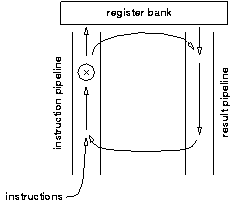
The counterflow pipeline neatly solves the problem of result forwarding. However it seems that the throughput of the processor is ultimately limited by the rate at which instructions can progress, and this is not likely to be particularly fast in view of the amount of comparison and arbitration logic required at each stage.
Hades is a proposed superscalar asynchronous processor in the early stages of design from Corrie Elston at the University of Hertfordshire [ELST95]. It is in many ways similar to a conventional synchronous superscalar processor; it has a global register bank, forwarding, and a complex (though in-order) instruction issuer. Its forwarding mechanism uses a central scoreboard to keep track of which result is available from where.
ECSTAC is an asynchronous microprocessor designed by Shannon Morton, Sam Appleton and Michael Liebelt at the University of Adelaide [MORT95].
ECSTAC is implemented using fundamental mode control circuits.
It is deeply pipelined with a complex variable length instruction format. It has 8 bit registers and ALU. The designers report that the variable length instructions and the mismatch between the address size and the datapath width made the design more complex and slower.
There is no forwarding mechanism within the datapath, and a register locking scheme is used to stall instructions until their operands are available.
TITAC is a simple asynchronous processor built by a group at the Tokyo Institute of Technology [NANY94]. It is based on the quasi delay insensitive timing model and so has to use dual rail signals to encode its datapath; this results in about twice as many gates in the datapath compared to an equivalent synchronous datapath.
Architecturally TITAC is very straightforward with no pipelining and a simple accumulator-based instruction set.
ST-RISC is an architecture proposed by a group from the Israel Institute of Technology [DAVII93]. It is delay insensitive and uses a dual-rail datapath.
ST-RISC has a two stage fetch-execute pipeline and a 3-address register based instruction set.
FAM [CHO92] is a dual rail asynchronous processor with a RISC like load-store instruction set. It has a four stage pipeline but register read, ALU, and register write occur in a single stage eliminating the need for any forwarding.
STRiP was built by Mark Dean at Stanford University [DEAN92]. Its instruction set is that of the MIPS-X processor.
STRiP is included here even though it has a global clock signal and could be considered synchronous. It is unusual in that the speed of the global clock is dynamically variable in response to the instructions being executed, giving much of the advantage of an asynchronous system. The performance of STRiP is typically twice that of an equivalent synchronous processor.
By maintaining global synchrony STRiP is able to implement forwarding in the same simple way that synchronous processors do.
The processors described here can be divided broadly into two categories:
From the point of view of this work it is the second category that is more interesting. The lessons that each of these processors teaches us are
AMULET1: Asynchronous implementation of a commercially important processor is possible. Exceptions and interrupts are possible. The lack of forwarding and branch prediction are significantly detrimental.
AMULET2: Forwarding is possible in a simple pipeline.
NSR: Decoupling with fifos is easy, but perhaps too easy as it is detrimental to performance. An instruction set with explicit queues and decoupling is possible.
Fred: Multiple functional units can be used with a single instruction issuer, but the throughput will be limited by the issuer.
CFPP: An interesting though expensive general implementation of asynchronous forwarding.
Hades: Superscalar control of the style used by synchronous processors is applicable in principle to asynchronous processors.
ECSTAC: Variable length instructions are unpleasant to deal with.
STRiP: Global synchrony does not have to mean fixed frequency clock signals.