A gate-level implementation of the architecture and instruction set described in the previous chapter has been carried out using the hardware description language VHDL. This design is at a sufficiently detailed level that it could be used for a silicon implementation, but this has not been done and instead the correctness and performance of the design have been established by simulation.
The first sections of this chapter describe the choice of asynchronous design style used and the overall design methodology. Later sections describe the implementation of selected parts of the architecture: the instruction issuer, the result routing network and the functional units. These areas have been chosen as they illustrate the more interesting parts of the processor in terms of asynchronous design. The final section concludes by measuring the size of the complete design.
The term "asynchronous design" is very broad; it simply means not synchronous. Within this category there are design styles that differ from each other as much as they differ from synchronous design. This section briefly describes some of these styles and investigates their properties.
Underlying each design style is a timing model. The timing model specifies what assumptions the designer is allowed to make about the relative timing of events in the system.
There are three basic timing models [SEIT80]:
In the bounded delay model an upper and a lower bound is known for each gate delay.
In the speed independent model gate delays are assumed to be unbounded but finite, but wires are assumed to have zero delay.
In the delay insensitive model both gate delays and wire delays are assumed to be unbounded but finite.
In the progression from bounded delay to speed independence to delay insensitivity the designer is given less and less freedom in what he may build; all delay insensitive circuits are speed independent and all speed independent circuits work under bounded delay, but the converse is not true.
On the other hand this progression gives the designer increasing freedom in how the circuits may be constructed. In a delay insensitive circuit any interconnection of functionally correct components will operate as desired. For speed independence any collection of gates will function but wires must act as equipotential regions, that is all gate inputs driven by the wire must change together. Under the bounded delay model the designer must use gates whose delays are known to be within the limits of his delay assumptions.
This trade-off is an important one. A pragmatic designer may choose to use some combination of the different timing models in different parts of his system. For example when using full-custom tools to design at the layout level the delays in gates and wires can be accurately predicted. In this case it is reasonable to use a bounded delay timing model which allows the greatest choice of circuits. When designing at a more abstract level with less control over circuit geometry and capacitances accurate knowledge of gate delays may not be possible. Here the speed independent or delay insensitive model may be applied.
The structure of control circuits is often quite random in nature and automatic placement and routing tools are generally used. This gives the designer little control over propagation delays and consequently control circuits may be designed to be speed independent or delay insensitive.
Asynchronous control circuits are often built up from simple subcircuits that perform operations such as sequencing, merging, and selecting. Because these macromodules will be used many times the designer may choose to make a bounded delay internal implementation. This requires more effort and may require manual placement and routing (or at least manual verification after automatic placement and routing), but the bounded delay circuit may be significantly simpler than the alternative speed independent or delay insensitive circuit.
Datapaths are important for two reasons: firstly they comprise a large part of many designs so their efficient implementation is important. Secondly they have a very regular structure which can sometimes be exploited for timing purposes.
Datapath busses comprise a number of bits whose values are used together. When each bit of the bus has been computed by one stage of the datapath the next stage may start its operation.
Under the speed independent and delay insensitive timing models the individual bits may become valid at quite different times. Consequently it is necessary for each bit of the bus to encode three possible states: logical 0, logical 1 and "not yet ready". This is typically done using a "dual rail" encoding where two wires represent each bit.
A number of designs[FOOTNOTE] including the Caltech asynchronous processor, TITAC, and the earlier Tangram work [BERK91] used this dual rail encoding. These designs demonstrated the substantial overhead of a dual rail encoding in terms of area, power and possibly performance compared with a single rail datapath.
[FOOTNOTE] See section 4.4
Under the bounded delay timing model a different approach known as "bundled data" is possible. In a bundled data system the datapath uses a single wire for each bit like a synchronous datapath and provides a single timing signal. This timing signal is delayed by an amount guaranteed to be greater than the longest delay of any of the data bits. In this way the area is reduced compared with the dual rail implementation. However it is necessary to calculate and implement the necessary delays for the timing signal.
The previous section suggested that the bounded delay model is most appropriate for small circuits where the delays can be accurately predicted. Datapaths do not meet this criterion. However datapaths do have a very regular structure and so delays in all bits should be well matched. The timing signal's delay path may be implemented safely by adding an extra bit to the datapath and adding some suitable safety margin.
Communication between blocks in an asynchronous system typically uses pairs of wires called "request" and "acknowledge". Request indicates that an action should be initiated; acknowledge indicates that the operation is complete. In bundled data systems this request-acknowledge handshake also indicates the validity of associated data signals. This exchange is sometimes referred to as handshaking.
Two alternative signalling protocols have been proposed for handshaking using the request and acknowledge signals; these are the 2-phase and the 4-phase protocols.
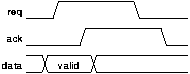
The 4-phase protocol is a return to zero protocol. The behaviour of the request and acknowledge signals and any associated data bus is indicated in figure 6.1. The rising edge of request indicates the validity of the data and the desire for the action to begin. The rising edge of acknowledge indicates that the data may become invalid and that the action has completed. The falling edges of request and acknowledge comprise the recovery phase of the protocol and perform no useful work[FOOTNOTE].
[FOOTNOTE] Other 4-phase protocols are possible; for example in the "long hold" protocol the data remains valid until after the falling edge of acknowledge. These alternative protocols may sometimes permit implementation optimisations.
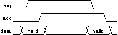
The 2-phase protocol is a non return to zero protocol. The rising edges of request and acknowledge indicate the start and end of data validity and the start and end of the required operation as before. However the handshake now finishes with the request and acknowledge signals both high. The subsequent falling edges of request and acknowledge indicate the next handshake as shown in figure 2.
The combination of 2-phase signalling and bundled data is proposed by Sutherland in his paper Micropipelines [SUTH89].
Arguments in favour of 2-phase signalling are that fewer signal transitions are required which reduces power consumption and that the lack of a recovery phase gives potential for faster operation. On the other hand advocates of 4-phase signalling suggest that 4-phase macromodule components are simpler and smaller than equivalent 2-phase components, giving both speed and power benefits.
The AMULET1 microprocessor was implemented using 2-phase signalling. Subsequent work [DAY95] has investigated the possibility of using the 4-phase protocol. The conclusion is that 4-phase is superior in terms of speed, power, and area; the AMULET2 microprocessor is being implemented using 4-phase signalling.
Interestingly the opposite conclusion has been drawn by the TAM-ARM project at Manchester which has implemented part of the asynchronous ARM using an ECL process. In this technology, which uses differential voltage signalling, the 2-phase protocol is preferred.
The SCALP design choices have been made with conventional CMOS implementation of the same type used by the AMULET processors in mind. Consequently the SCALP implementation uses 4-phase signalling[FOOTNOTE] with bundled data datapaths.
[FOOTNOTE] Section 6.3 describes one case where the 2-phase protocol was found to be superior.
The overall design flow was as follows:
Instruction set design.
Assembler and instruction set simulator written in `C'.
High-level behavioural simulation written in VHDL.
High-level simulation verified against `C' simulation using general test programs.
Simple gates and basic asynchronous elements modelled using behavioural VHDL.
More complex asynchronous macromodules designed in terms of basic elements by hand or with simple asynchronous synthesis tools.
Gate level implementations of functional units and other blocks designed.
Blocks verified against `C' simulation using block level test programs.
Blocks combined to form complete gate level processor model.
Processor model verified against `C' simulation using general test programs.
Processor model evaluated using "real" programs and specially developed test sequences.
The primary tool used in the implementation of SCALP has been the hardware description language VHDL. VHDL has a number of characteristics which make it ideal for this task:
Good range of high-level types and constructs suitable for abstract behavioural modelling.
Good low-level features for gate-level modelling.
Good modularity suitable for a large project.
Event based simulation model suitable for asynchronous logic.
Fast and reliable simulators.
Good support from other CAD software.
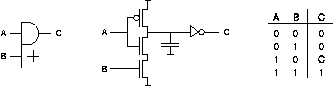
The set of basic gates used is based on the AMULET Low Power Cell Library [FARN95]. It includes conventional gates such as and, or, nand, nor, and xor as well as special asynchronous gates such as Muller C gates. An example C gate's symbol, simplified implementation using dynamic logic, and truth table are shown in figure 1; 17 different types of C gate are used in the design. C gates are the main state holding elements in this type of asynchronous circuit.
More complex asynchronous macromodules were built from these basic gates. The designs come from three sources:
The AMULET2 design.
Designs synthesised from choice free signal transition graphs using the program FORCAGE [KISH94]. FORCAGE is less sophisticated than some of the other synthesis programs and cannot be applied to many of the macromodules because they include choice.
Designs carried out by hand.
The macromodules used are described in table 6.1.
Name		Function

once_or_twice	For each input handshake perform either one or two
		output handshakes depending on the value of a
		condition input.

twice		For each input handshake perform two output handshakes.

cond		For each input handshake perform either zero or one
		output handshake depending on the value of a
		condition input.

cond_undec	As cond, but input acknowledge is not deasserted until
		output acknowledge is deasserted i.e. there is no
		decoupling between input and output.

seqj2		For each input handshake perform a handshake on each
		of the two outputs in turn.

seqj3		For each input handshake perform a handshake on each
		of the three outputs in turn.

seqs2		As seqj2 but second output request is not asserted
		until first output acknowledge is deasserted.

seqs3		As seqj3 but second and third output requests are not
		asserted until first and second output acknowledges
		(respectively) are deasserted.

cond_pipe_merge	When condition input is asserted, wait for both input
		requests to be asserted before asserting output
		request.  When condition input is not asserted, wait
		only for first input request.  See figure 4.11.

pipe_merge	Wait for both input requests to be asserted before
		asserting output request.

sel2		Send each input handshake to one of the two outputs
		depending on the value of the condition input.

steer2		As sel2 but without acknowledge signals.

call2		Handshakes on either of two mutually exclusive inputs
		cause a handshake on the output.
The majority of the macromodules carry out quite simple functions, such as sequencing or selection of events. Undesirable complexity results from two things:
What to do with the acknowledge signals. Often the logic required to generate the output request signal is straightforward, but more complexity is associated with storing some internal state so that the correct acknowledge signals are subsequently generated.
What to do with the return to zero phases of the 4-phase protocol. Generally a simple approach to the return to zero phases is possible but it has poor performance. The alternative is to add additional components to "decouple" the return to zero phases. These additional components may have the effect of slowing down the forward logic. Which solution is best in a particular application is hard to evaluate and depends on the speed of the environment.
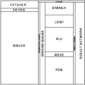
Figure 6.4 shows the top-level of the SCALP implementation. This section presents a brief overview of the function of each of the blocks in the design. The following sections consider the more detailed implementation of some of the more interesting areas.
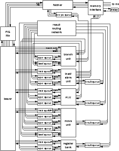
The SCALP model has a single memory port which is shared by instruction fetch and load/store accesses. The memory interface is responsible for arbitration and multiplexing between the load/store unit and the fetcher for access to the memory.
The fetcher contains the program counter. When a free space is present in the FIG fifo the fetcher reads the next FIG[FOOTNOTE] from memory using the memory interface. The 64 bit FIG is fetched in two cycles as the memory interface is only 32 bits wide.
[FOOTNOTE] FIG: Five Instruction Group
Branch target addresses are sent to the fetcher by the branch unit. If a space is available in the FIG fifo but no new address has been sent from the branch unit then the fetcher increments the last program counter value and sends this to the memory. The block has to arbitrate between the arrival of a new address from the branch unit and the dispatch of an incremented program counter value.
The FIG fifo is a three stage queue that stores FIGs between the fetcher and the issuer. Its purpose is to provide decoupling between the two units so that neither unit suffers blocking or starvation; for example if the load/store unit gains access to the memory interface then the fetcher will be unable to supply new FIGs, but due to the FIG fifo the issuer will be able to continue to operate.
The issuer decodes the functional unit identifier bits in the instructions in incoming FIGs and distributes them to the appropriate functional units via the instruction queues.
The two deep instruction queues provide decoupling between the instruction issuer and each of the functional units.
The operand queues store values that have been computed by previous instructions and sent to their next instructions by explicit forwarding. The values remain in the queues until they are matched with instructions. The queues are each two deep.
The branch unit executes branch instructions. For conditional branch instructions it receives comparison results from the ALU via the CBRAN boolean queue. For the computed branch instruction it receives a target address via the BRC queue. It sends target addresses to the fetcher via a single stage queue.
Most branches are relative to the current program counter value. The branch unit contains an adder which performs this calculation. The current program counter value is provided to the branch unit for this purpose with each instruction from the issuer.
The branch unit has no instruction queue. This is so that the branch unit can acknowledge to the issuer to indicate whether each branch has been taken or not. It is the responsibility of the instruction issuer to skip over any incorrectly fetched instructions between a taken branch and the branch target.
The branch and link instruction causes the unit to send the address of the instruction following the branch to the move unit's LINK queue. This is used to effect a subroutine call.
The ALU executes arithmetic, logical and comparison instructions. Arithmetic operations are carried out by a completion indicating ripple carry adder. Logical operations are carried out by a simpler piece of logic with a matched delay path. The results of arithmetic and logical operations are sent to the result network.
Comparisons are performed by either subtracting or exclusive-ORing the operands using the normal arithmetic and logical blocks. The result is then tested for equality to zero or the adder's carry out is tested. This means that comparison for equality is faster than a magnitude comparison as the later requires only an exclusive OR rather than a subtract. Comparison results are sent to either the branch unit's CBRAN input or the move unit's CMOVE input.
The load/store unit executes load and store instructions. It accesses the memory via the memory interface. The block contains an adder which adds a displacement provided in the instruction to an address provided by the MEMA queue. Store data is provided by the MEMD queue. Load results are sent to the result routing network.
The move unit executes four special purpose instructions. DUP duplicates its operand, sending the two copies to any two operand queues. SEQ sequentialises two operands, sending them to a single destination in a deterministic order. CMOVE is a conditional move instruction; either one of its input operands is sent to the destination under the control of a boolean input from the result of a comparison. The MVLINK instruction transfers a value from the LINK queue to some destination, for example a leaf subroutine can return by using MVLINK to send the link value back to the branch unit.
The register bank contains a 32 entry register file and executes READ and WRITE instructions that access it. WRITE data is provided by the REGD input. READ results are sent to the result network.
The result queues provide a single stage of decoupling between the functional units and the result routing network. This decoupling helps to prevent functional units from blocking when the result routing network is temporarily busy.
The result routing network transfers the results of instructions from the result queues to the operand queues. Each functional unit copies the destination address from its instruction to the result output to accompany the result data. The result routing network uses this address to select one of the eight operand queues.
The instruction issuer is one of the key parts of the SCALP design. It accepts five instruction groups (FIGs) that have been fetched from memory and sends the individual instructions to the five functional units. Each interface uses a 4-phase bundled data protocol. The issuer is decoupled from the fetcher and the functional units by fifo queues.
Each instruction within the FIG contains three bits that indicate to which functional unit it must be sent (figure 5.3). The issuer must study these bits for each instruction and select the appropriate output.
The operation is made more complex by the variable length instructions and the special treatment of branch instructions. To clarify this description a simplified design excluding these features is presented first and these additional aspects are added later.
One functionally correct though unsatisfactory implementation of the instruction issuer is shown in figure 6.5.
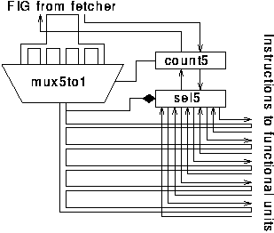
This circuit works as follows: when a FIG arrives from the fetcher, the count5 block and multiplexor split it into its five constituent instructions which are considered in turn. The three bits that indicate which functional unit the instruction is for are split off from the rest of the instruction and control a five way select element. The outputs of this select are requests to each of the functional unit queues.
The problem with this solution is that it is too sequential. In a pipelined processor it is essential that no part of the system becomes a consistent bottleneck; the throughput of each stage must be balanced. The memory interface can fetch several instructions at once and the five functional units can operate in parallel. This instruction issuer can issue only one instruction at a time and unless it can be made to operate five times as fast as the other parts of the system - which is unlikely - it will become a bottleneck.
The design of the instruction issuer must therefore incorporate parallelism, allowing several incoming instructions to be considered and issued to different functional units simultaneously.
Note that although the order in which instructions for one particular functional unit must arrive at that functional unit is fixed, the order in which instructions are issued between the functional units may vary. For example, if a FIG contains five instructions for these functional units:
	 0   1   2   3   4
	F0  F0  F2  F2  F1
then initially instructions 0, 2 and 4 can be issued to functional units F0, F2 and F1 respectively. Subsequently instructions 1 and 3 can be issued.
The boundaries between FIGs are also unimportant. For example if two FIGs contain instructions for these functional units:
	 0   1   2   3   4
	F0  F0  F0  F0  F0
	F1  F1  F1  F1  F1
then the issuer may choose to issue instruction 0 in the first FIG to functional unit F0 and simultaneously instruction 0 in the second FIG to functional unit F1.
A good solution will trade off the performance benefits of these forms of out-of-order issue against their implementation cost. This trade-off is considered further in section 6.4.6.
The proposed solution makes use of a 5 by 5 crossbar switch to allow unrestricted connections between each instruction in the FIG and each functional unit. The incoming FIGs are stored in a "forked fifo"; this is an asynchronous fifo queue whose input is controlled by a single request/acknowledge pair and whose output has separate request and acknowledge signals for each instruction. This arrangement means that once an instruction has been issued then it can be acknowledged and removed from the output of the fifo making the instruction behind it in the next FIG visible and eligible for issue.
Control is then divided up into one unit corresponding to each of the functional units. These units "watch" the instructions at the front of the FIG fifo and when they see an instruction for their functional unit they activate the appropriate switch in the crossbar and send a request to the functional unit.
This arrangement is shown in figure 6.6 (connections between the controllers and the crossbar are omitted for clarity).
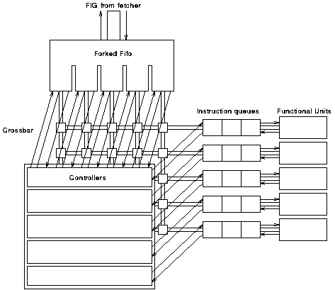
Each functional unit controller can see the following information about each instruction at the front of the FIG fifo:
From the state of the request and acknowledge signals, whether any valid instruction is present.
From the decoded functional unit bits in the instruction (the "for me" signals) whether this instruction is for this functional unit.
On the basis of this information the functional unit controller must choose which if any of the instructions it may issue at this time:
If none of the instructions is "for me" and "valid" then it can do nothing.
If one of the instructions is "for me" and "valid" then that one may be issued, unless a preceding instruction is not valid in which case the controller must wait to see if it is "for me" first.
If more than one instruction is "for me" then the first one in program order may be issued.
Unfortunately the information described above is not quite sufficient because of the way that the FIG fifo works. Consider the following two cases:
	 0   1   2   3   4
	F0  F1  F0  F1  F2
	F0  F1  F2  F3  F0

	 0   1   2   3   4
	        F0  F1  F2
	F0  F1  F2  F3  F0
In the first case the front row of the FIG fifo is full. In the second case the first two instructions from the front FIG have already been issued making the first two instructions from the second FIG visible.
Note that in both cases the instructions visible to the controllers are the same: F0, F1, F0, F1, F2. Consider the controller for functional unit 0. In the first case the correct behaviour is for it to issue instruction 0. In the second case the correct behaviour is for it to issue instruction 2. With the information described above it is not able to distinguish these two cases.
Here is another example:
	 0   1   2   3   4
	F0  F1  F0  F1  F2
	F0  F1  F0  F2  F2

	 0   1   2   3   4
	F0  F1  F0  F1
	F0  F1  F0  F2  F2
Once again the instructions visible to the controllers are the same: F0, F1, F0, F1, F2. Consider the controller for functional unit 2. In the first case the correct behaviour is for it to issue instruction 4. In the second case the next instruction in program order for functional unit 2 is instruction 3 of the second FIG, an instruction which is not yet available for issue, so the controller must do nothing.
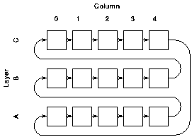
To solve these problems further information must be made available about the instructions at the head of the FIG fifo. A modulo-3 counter controlled by the request and acknowledge signals is associated with each column of the FIG fifo. The controllers see the states of these counters and are able to tell which instructions belong logically before others. The letters A, B, and C are used to indicate the state of the counter. This is referred to as the "layer" in which the instruction belongs; this is orthogonal to the rows and columns of the crossbar.
The algorithm that each controller has to implement is then as follows:
At reset, the "current column" is column 0 and the "current layer" is layer A
If the instruction in the current column is not valid (i.e. request is not asserted; it has not arrived) then wait.
If the instruction in the current column is for the previous layer then wait.
If the instruction in the current column is for the current layer and it is for this functional unit then issue it.
If the instruction in the current column is for the current layer but it is not for this functional unit then consider the next instruction.
If the instruction in the current column is for the next layer then consider the next instruction.
When the instruction in column 4 has been considered, go on to column 0 of the next layer.
The algorithm is described here in a sequential fashion, but it could be implemented in parallel using priority encoders and similar structures. Several possible approaches were considered and eventually one based on token passing was chosen.
The principle of operation is this: for each column and each layer a block of logic precomputes what it would do if this column and layer were "current". The possible actions are to wait, to consider the next instruction, and to issue this instruction. These precomputations can be carried out for all columns and layers in parallel. A "token" is then passed between the blocks. When a block holds the token the column and layer that it represents are the current column and layer. When the token arrives the block performs one of three possible actions:
If the action is to wait, the token is kept by the block. Eventually conditions will change (for example the input will become valid) causing the action to change to one of the others.
If the action is to consider the next instruction then the token is passed to the next block.
If the action is to issue this instruction then the appropriate crossbar switch is activated and a request is sent to the functional unit. When the functional unit sends an acknowledge then an acknowledge is sent to the FIG fifo and the token is passed to the next block.
The organisation of the blocks and the token's path between them is shown in figure 6.7. Note that there is one token and associated structure of this type for each functional unit.
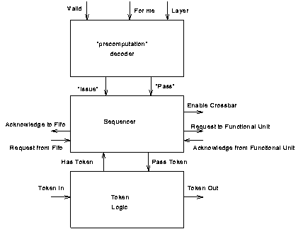
Internally each block is divided into three sub-blocks as shown in figure 6.8. The decode block performs a combinational function to decide which of the three actions wait, pass, or issue should be carried out. The sequence block is an asynchronous sequential circuit that operates according to the required action in response to the arrival of a token, driving the functional unit and crossbar outputs when necessary. The token block is responsible for receiving tokens from the previous stage and sending them to the next stage under control of the sequence block.
For reasons described in section 6.1.3 the majority of the SCALP design has been carried out using the 4-phase signalling protocol. In the case of the token block a 4-phase implementation was carried out, but it was subsequently found that a 2-phase implementation can be both smaller and faster[FOOTNOTE]. The design is shown in figure 6.9. Note that it is only the token_in and token_out signals that are 2-phase; the has_token and pass_token signals are 4-phase.
[FOOTNOTE] One reason why the 4-phase implementation was more complex is that it needed acknowledge signals for the tokens. The 2-phase circuit manages without them.
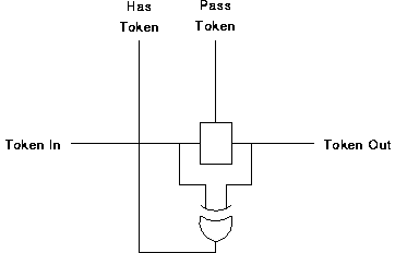
Operation is as follows: when no token is present, the input and output are the same and the output of the XOR gate is 0. When a token arrives on the input, the XOR gate output becomes high asserting has_token. When pass_token is asserted the latch is opened and the transition representing the token is passed to the output. Both inputs to the XOR gate are equal once more and has_token returns to zero.
Note that with this circuit pass_token may be asserted before a token has arrived, indicating that the token should be passed on as soon as it arrives. In this case the token may pass from block to block with each block imposing only a single gate delay.
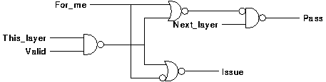
The purpose of the decode block is to decide on the basis of the for_me, layer, and valid signals what should happen when the token arrives. It has two outputs, "issue" and "pass". "issue" indicates that when the token arrives the instruction in this column should be issued and the token passed on. "pass" indicates that when the token arrives it should be passed on without issuing anything. If neither is asserted, when the token arrives nothing should happen i.e. the block waits. The function that the block has to perform is described in table 6.2.
Inputs			Interpretation			Outputs

Valid	Layer	For_me					Issue	Pass

X	Previous
		X	Can't see the instruction
			we want; wait			0	0

0	This	X	Must wait until this
			instruction is valid to see if
			it is for me; wait		0	0

1	This	0	This instruction not for me;
			pass				0	1

1	This	1	For me; issue			1	0

X	Next	X	The instruction that was here
			has been issued by another
			controller;  pass		0	1
This function must be implemented so that there are no glitches on the issue and pass outputs for any valid input change sequences. An implementation is shown in figure 6.10.
The function of the sequence block is to carry out the action indicated by the decode logic when the token arrives. This means either passing the token on by asserting pass_token or issuing an instruction.
Passing is straightforward: pass_token is asserted in response to pass. Issuing the instruction involves more steps and some choices. For example, at what point should the token be passed on? Can it be passed when issuing starts or must it wait until it has completed? If the token is passed when issuing starts performance will be improved but subsequent blocks must check that this issue has finished before starting to issue themselves. This solution takes a simple approach as shown in figure 6.11.
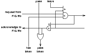
The four input Muller C element[FOOTNOTE] generates the request signal to the functional unit. It is asserted when the following four conditions hold:
[FOOTNOTE] Asymmetric Muller C elements are represented here by a gate symbol with extensions to one or both sides. Inputs joining the body of the gate take part in both rising and falling transitions of the output. Inputs joining a side marked with a + or - take part in only the rising or falling output transitions respectively.
The issue signal from the decode block is asserted.
The acknowledge signal from the functional unit is not asserted, i.e. any previous issue to this functional unit has completed.
This block has the token.
The request signal from the FIG fifo is asserted (this will always be the case when the issue signal from the decode block is asserted).
When the functional unit's instruction fifo has accepted the instruction it will assert its acknowledge signal. The role of the second Muller C element is to select only those acknowledge signals that result from requests from this block. When its output is asserted two things happen:
The acknowledge signal to the FIG fifo is asserted.
The token is passed on.
The top Muller C element's output is deasserted when the acknowledge to the FIG fifo and the token passing have completed. This is detected by the request from the FIG fifo and has_token both being deasserted.
Branch instructions complicate the instruction issuer in two ways:
When a branch instruction is taken, instructions between the branch and the branch target must be disposed of. This task is the responsibility of the instruction issuer. Branch targets are identified as such by means of an additional bit per instruction introduced by the fetcher. The branch unit indicates whether a branch has been taken when it acknowledges the instruction.
In order to not issue instructions that should have been disposed of, controllers for other functional units must not consider instructions beyond the instruction currently being considered by the branch unit's controller.
The first of these complications is dealt with as follows:
The branch unit controller has an additional token signal between each block. The existing signal transfers "look" tokens and the additional signal transfers "delete" tokens.
When a "look" token is received the block considers the current instruction in the normal way. If the instruction is issued and the branch unit acknowledges indicating that the branch was not taken then a "look" token is passed to the next block as normal.
If the branch unit acknowledges indicating that the branch was taken then a "delete" token is passed to the next block.
When a "delete" token is received the block studies the bit indicating whether this instruction is a branch target. If it is not a branch target then the instruction is discarded by asserting acknowledge to the FIG fifo. A "delete" token is then passed to the next block.
If a "delete" token is received and the current instruction is a branch target then the instruction is considered as normal and a "look" token is passed to the next block.
The second complication of preventing other controllers from overtaking the branch controller is dealt with as follows: the token block in each block contains additional logic that delays the arrival of a new token when the branch unit controller has a token in the same column and layer. At reset the branch unit controller is given a "head start". In this way the other controllers all follow behind the branch controller.
Each of the five chunks of a FIG may be either an instruction or an immediate value associated with the previous chunk. Which instructions have immediate chunks is indicated by the FIG's control field (see figure 5.9).
Three of the functional units (ALU, load/store, and branch) accept instructions with optional immediates. These functional units have double-width instructions queues that can accept one or two chunk instructions.
There are three main ways in which the instruction issuer must be extended to deal with the variable length instructions:
The crossbar is extended to allow each of the input chunks to be directed to either the instruction or the immediate part of each instruction queue.
The control field is decoded to provide an additional bit for each column of the FIG fifo indicating if the instruction in this column has an associated immediate. Each decode block is then extended to decode two new actions: issue with immediate and pass with immediate (in addition to the existing issue, pass and wait). The sequence blocks are extended to deal with these extra actions.
The token logic is extended to allow tokens to be passed to either the next block or to the block after next. This is required so that immediate fields are skipped over and not treated as instructions. Additional token signals are required between the blocks. Incoming tokens are merged with an XOR gate. Outgoing tokens can be steered to either of the next two blocks.
The effect of these changes is significant both in terms of the size and the performance of the issuer. This is studied further in the next section.
As with many types of design the performance of the instruction issuer is determined by its architectural performance and by its implementation performance. Architectural performance refers to the number of instructions that can be issued per cycle. Implementation performance refers to the time taken per cycle.
The sequential issuer of figure 6.5 operates at 1 instruction per cycle. The parallel issuer described here can operate at up to 5 instructions per cycle. However this performance can only be achieved when the instructions within each FIG are evenly distributed between the functional units. When the instructions are not evenly distributed the performance will be limited by the controllers for the more heavily used functional units.
Other issuer architectures are possible; in particular it is possible to make the issuer wider or narrower so that more or fewer than five instructions can be considered at a time.
A simulation has been used to measure the performance of the issuer described here for different instruction mixes and for different widths of instruction issuer. The results of the simulation are shown in table 6.3 and figure 6.12.
Organisation		Instructions		Performance /
						chunks per cycle

Sequential issuer	Any			1.00
(figure 6.5)

As described:		Best case		5.00
5 columns

			Evenly distributed	2.92
			random instructions

			qsort program		1.86
			(see section 7.1.1)

2 columns		Evenly distributed	1.67
			random instructions

3 columns					2.23

4 columns					2.63

5 columns					2.92

10 columns					3.78

15 columns					4.27

20 columns					4.58

25 columns					4.83
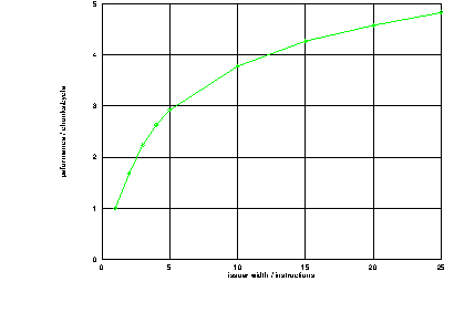
It can be seen from these results that the issuer's performance could be substantially increased by increasing the number of instructions that are considered at a time, though this would be at the cost of substantially increasing its size. If the instruction issuer was a bottleneck in the processor as a whole then this may be an attractive option. Subsequent results (section 7.3) will show that this is not the case and that other parts of the processor limit its performance.
This section briefly compares the cycle times of the sequential issuer of figure 6.5, the simplified issuer described in sections 6.4.2 and 6.4.3 and the issuer as implemented with additional logic for branch instructions and variable length instructions.
The sequential issuer has not been modelled at gate level but an estimate of the cycle time is around 8 gate delays (GD) per instruction. This is equivalent to 40 GD per instruction per functional unit. This does not allow for branch or variable length instructions.
The simplified parallel issuer's cycle time would be as little as 12 GD per instruction per functional unit if its performance was limited by the speed at which tokens are passed from block to block. In practice the critical path lies from the output stage of the FIG fifo, through the modulo-3 counters to the decode blocks, through the sequence blocks in issue mode to the input stages of the functional unit instruction queues, and back through the sequence blocks to the FIG fifo acknowledge. This limits the cycle time to around 24 GD per instruction per functional unit.
The performance of the issuer with support for branch instructions and variable length instructions is measured in detail in section 7.3.1. Its cycle time is at best 54 GD per instruction per functional unit.
The difference between the 24 GD cycle time of the simplified issuer and the 54 GD cycle time of the real issuer can be attributed to the additional complexity of dealing with branches and variable length instructions.
The result routing network transfers values from the functional unit outputs to the operand queues of other functional units. Each value has associated with it a bit indicating its width, byte or word, and three bits indicating its destination. The routing network has four inputs - one from each of the functional units except the branch unit - and eight outputs.
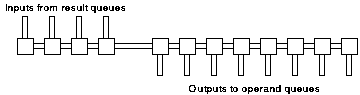
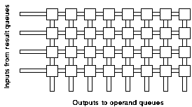
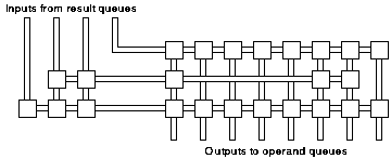
As with the instruction issuer an important initial question is the degree of parallelism that is required. A simple sequential design (figure 6.13) could be implemented that processes only one value at a time. At the other extreme a fully populated crossbar (figure 6.14) could be used to provide the greatest performance but with significant hardware cost. Initial analysis suggested that a balanced solution would lie between these two extremes. The proposed structure is shown in figure 6.15.
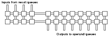
The datapath comprises two shared busses. Each of the four network inputs is connected to both busses by a tri-state buffer, and each bus is connected to each output in the same way.
Control is divided into two parts associated with the input side and the output side respectively. The input side is responsible for arbitrating between the four inputs and granting access to the shared busses. The output side is less complex; it studies the destination specifiers on the busses and activates tristate connections and output requests as necessary.
A complex arbiter is required to control the input side of the controller. It has four request inputs corresponding to each of the inputs to the network. Associated with each request input are two grant outputs. In response to a request input being asserted one of the grant outputs will eventually be asserted. This indicates that that input may drive the associated bus. The grant output will remain asserted until the request is deasserted. No more than one input may be granted use of each bus at any time.
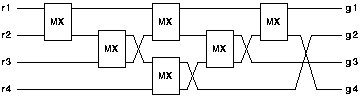
The basic arbitration element available for the design is the two input mutual exclusion element. This element has two request inputs and two grant outputs. When one request input is asserted the corresponding grant output is subsequently asserted. When both request inputs are asserted simultaneously the element resolves any metastability internally and eventually asserts exactly one grant signal. It is guaranteed that no metastable activity will be observed on the output signals, though the arbiter may take an arbitrarily long time before asserting either signal.
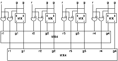
From these two input mutual exclusion elements it is necessary to construct a four input mutual exclusion element. One such element will be associated with each bus in the controller. The circuit used for this purpose is shown in figure 6.16.
The operation of the overall controller is as follows: When a request is received, the corresponding requests to both four way mutual exclusion elements are asserted. Eventually one or other (or both) will assert the corresponding grant signal. A two way mutual exclusion element is used to arbitrate between the two grant signals so that only one of the grant inputs is asserted. The request to the other four way mutual exclusion element is then released.
The circuit used is shown in figure 6.17.
The network organisations considered here are all symmetric, i.e. all outputs have equal access to all busses. More efficient solutions may be provided by networks that are biased towards some patterns of communication and against others. Figure 6.18 shows such an arrangement. One input has exclusive use of a bus. Two other busses are shared by two other inputs, with the fourth input given access to only one of them. On the output side two of the busses are connected to all outputs but the other has limited connectivity.
The interconnections in a scheme of this sort would have to be based on analysis of network usage by benchmark programs.
Although each of the five functional units performs a different function, in terms of structure they have much in common.
The interfaces to the units are similar. Each has an input for instructions from the issuer and for one or more operands from the result network. They also have similar outputs to send results to the result network.
Internally, the functional units are divided into datapath and control sections as shown in figure 6.19. The datapaths comprise multiplexors, adders and other logic connecting the inputs and outputs under the control of various signals from the control logic.
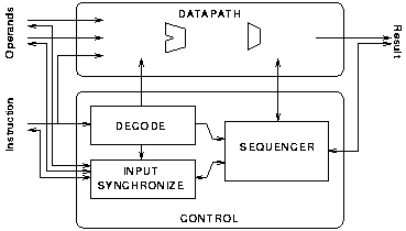
The structure of the control logic in each functional unit is similar; it comprises instruction decoding, input synchronisation and sequencing.
The decoder studies the instruction and generates a number of control signals; some of these go to the datapath. Other signals indicate which of the various operands are needed by this instruction.
The role of the input synchroniser is to establish when all of the necessary operands and the instruction have arrived. When this occurs it indicates the fact to the sequencer.
The sequencer is responsible for activating any sequential logic in the datapath such as an adder and for sending the result to the output; this part of the design varies substantially from one functional unit to another.
As an illustration, figure 6.20 shows the arrangement of the sequencer for the branch unit.
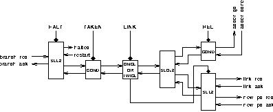
Its operation is as follows: the instruction is decoded to provide the HALT, TAKEN, LINK and REL inputs which indicate that the branch is a halt instruction, is taken, is a branch and link instruction and is a relative branch respectively. When any necessary operands have arrived the branch_req input from the input synchroniser is asserted.
The first block is a two-way select block that deals with the HALT instruction. For halt instructions the external output "halted" is asserted and the sequencer awaits the "restart" input before continuing.
For all other instructions the request is passed to the next block. For untaken branches the conditional block returns the request directly to the acknowledge. For taken branches the request proceeds to the next block.
Most branch instructions execute in a single "cycle". The exception is the branch and link instruction which uses one cycle to compute the target address and a second cycle to compute the link address (either the address of the current instruction or the address of the current instruction plus one). The "once or twice" block cycles its output twice for link instructions and once for others.
The next block is a simple sequencer that activates each of its two outputs in turn. The purpose of the upper (first) output is to activate the adder when necessary. The adder is only required by relative branches so a second COND block enables it only in this case.
The second output of the sequencer is used to send the result from the datapath to its destination. This may be either the link address queue for the link cycle of a branch and link instruction or the new PC queue of the fetcher for other cycles. An additional output from the earlier once or twice block controls a select block that steers the signal to the appropriate output.
The number of basic gates modelled in the VHDL code has been counted and is broken down by gate type in table 6.4. The total number of components is around 9,500. The number of gates used by each block is shown in table 6.5[FOOTNOTE].
Count	Gate		Description

220	and2		AND gates

131	and3

1	and4

181	dffr		D-type flip-flop

1334	inv		Inverter

7	mc101		Muller-C elements; first digit is
			number of symmetric inputs, second is
			number of positive-only inputs, third
			is number of negative-only inputs.  R
			suffix indicates global reset.  In
			a VLSI implementation some of the larger
			gates would be implemented from
			several smaller components.

6	mc101R

6	mc102

3	mc102R

1	mc103

174	mc110

1	mc110R

10	mc111

10	mc112R

195	mc120

12	mc120R

98	mc2

24	mc201R

90	mc220

25	mc2R

1	mc3

75	mc320

18	mutex		Mutual exclusion (arbitration) element

2397	nand2		NAND gates

551	nand3

42	nand4

497	nor2		NOR gates

66	nor3

59	nor4

454	or2		OR gates

70	or3

15	or4

1	ram32x24	RAM blocks (register bank)

1	ram32x8

1365	TL		Transparent latches

82	TLR

5	TLsetR

838	tridrv		Tri-state driver

32	xnor2		Exclusive OR gates

402	xor2
Block			Gates		Proportion

Issuer			4165		39 %

( of which Switches	550		5 %

Control			3615		34 % )

Result Network		1194		11 %

Register Bank		1158		11 %

ALU			1090		10 %

Operand Queues		624		6 %

Branch Unit		548		5 %

Load/Store Unit		488		5 %

Fetcher			422		4 %

Move Unit		215		2 %

FIG Fifo		228		2 %

Instruction Queues	176		2 %

Result Queues		168		2 %

Memory Interface	106		1 %
[FOOTNOTE] In table 6.5 the RAM part of the register bank is counted as only two components. To provide a fairer idea of the register bank's relative size in table 6.6 an estimate of the equivalent number of components is given.
The relative sizes of the various blocks are indicated in figure 6.21.
The total number of transistors in the design is approximately 64,000. This is compared with the sizes of AMULET1 and the ARM6 processor in table 6.6.
Processor	Transistors

SCALP		64000

AMULET1		54000

ARM6		34000
Next Chapter