
APT research areas
The AMULET2e microprocessor
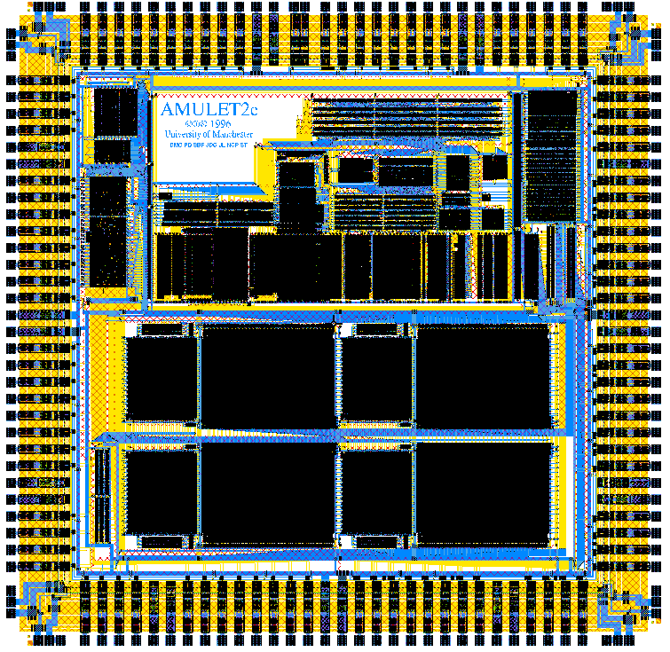

This is the final layout of the AMULET2e microprocessor, the second generation asynchronous ARM processor.
AMULET2e is a reimplementation of AMULET1. It features an AMULET2 processor core for Embedded applications, and includes on-chip memory which may be used either as cache or memory mapped RAM.
The microprocessor core is visible at the top of this picture with the 32-bit data path running horizontally. This comprises the address unit (swollen by the branch target cache) the register bank (with the 'tower' of its decoders and locking logic above it) and the execution unit to the right, all laid out as full custom silicon. Above the execution path is the majority of the control logic laid out from PLAs and standard cells.
The 4Kbytes of cache comprise the four identical 1Kbyte blocks below the processor. These each contain a RAM and a pitch-matched CAM (the smaller block).
The remaining logic blocks are standard cell units which provide the bus interface, some address decoding and a number of configuration registers allowing the various processor features to be tested and their effects measured.
Features include:
- Four phase micropipeline control circuits
- Power saving latch designs
- Load and register forwarding
- Branch target prediction
- "Sleep" mode
- Self-timed cache
- Dynamic external bus sizing
- Direct interface to commodity memory devices
- 0.5 µm, 3 layer metal process
- Core size 5mm x 5mm; die size 6.5mm x 6.5mm
A datasheet is available, as are several academic publications.
AMULET2e "taped out" 11/7/96. It was fabricated by VLSI Technology Inc.
We can't give a cycle time of course, because no two cycles are the same length, but things look to be around/over 40MIPs at present. That may change though (hopefully upwards). With a standard ARM compiler (not optimised for this implementation) 66kDhrystones have been achieved simulating 'typical' silicon.
AMULET2e returned from fabrication on 1/10/96. It ran a single instruction loop the same day and successfully communicated using the standard ARM "Demon" monitor software at 12.00 BST on Wednesday 2nd October 1996. Further software investigation is indicating that performance is very close to the predictions from simulation.
Initial measurements of performance depend on how the system is configured and which features are enabled. The fastest configuration for the Dhrystone benchmark is using the internal RAM as a memory mapped store rather than as a cache. This yields 74kDhrystones, equivalent to 42 Dhrystone MIPS. The power consumption of the processor core (excluding the pad drivers) is 150mW.
This performance (at 3.3V) is comfortably greater than ARM7 but somewhat behind ARM8. The power/performance looks to be comparable with ARM8. When the processor is halted the power consumption drops radically, to 3µW if the on board timer (which includes DRAM refresh) is not in use.
Also interesting are the EMC results. The figures below show graphs of the radiation from the AMULET2e test card (left/above) and an ARM6 PIE card, both running the Dhrystone loop under as similar physical conditions as possible. The AMULET2e clearly shows less harmonic noise and also a lower background emission level. The spectrum is from 30-1000 MHz.
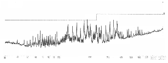
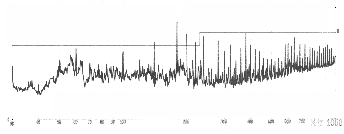
(Apologies for the low image quality; the scales are the same in each figure.)
AMULET2e bibliography
The AMULET2e development was supported by the OMI/DE-ARM project. The designers wish to acknowledge this support from the CEC.