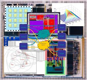
Vision Statement
Communication Centric Circuit Design
Simon Moore, University of Cambridge
15th November 2004
Background
Electronics is at the cusp of change. For the last 60 years, digital gates have been costly to produce and limited the performance. We are now entering an era where the wires, which were once almost free, being the cost and performance limiter. This trend has well documented in the International Semiconductor Industry Association (ISIA) roadmap which clearly identifies step change needed in circuits and associated design techniques. They also identify spiralling design complexity, escalating power densities and associated thermal problems. Despite this clear roadmap, even giants like Intel have been caught off guard. Intel recently cancelled their five year development programme for the Tejas processor since they were unable to reduce power density to a practicable level.
The need for a design revolution
Movement of data around a chip already dominates the power budget (computation is almost for free), so why do we continue to focus on the computation and sequencing of data rather than the efficient movement of data? On a now pedestrian 180nm CMOS process one typically requires a buffer that is 400 times larger than the minimum in order to drive just 1mm of on chip wire. Minimising data movement, and the amount of data being moved, can dramatically improve the power efficiency.
Managing design complexity is also vital as the cost per transistor continues to plummet. Clean interfaces and standardised communication mechanisms would greatly assist the use of IP blocks. Breaking a design into discrete blocks with a common interface could allow far more hierarchical and thorough verification.
Relevance to UK Industry
The UK plays a leading role in electronic design, as indicated by the recent House of Lords report on Chips With Everything. The UK has been particularly successful in the embedded systems market when power efficiency and fast time to market are key criteria. To stay ahead we need to embrace the technological and architectural design challenges for large systems-on-chip.
Challenges
There are a number of challenges. Specific communication centric circuit design, we need to develop:
- • Communication centric architectures for chip wide and chip-to-chip data movement
- • Standards for communication mechanisms to allow rapid integration of IP blocks
- • Verification techniques for on-chip communication mechanisms and interfaces
- • Circuit level techniques for efficient movement of data
- • Circuit level techniques for efficient data synchronisation (clocks or asynchronous approaches)
- • Hardware description languages that allow design to be focused on data-flow rather than computation
Each of these areas is huge and can be broken down into smaller projects.
There are also more general challenges:
- • Building robust and documented tool flows
- • Educating engineers to enable them to design more complex systems using new techniques

