
APT research areas
A Vision for Microelectronics: Making Measurements
David R. S. Cumming
University of Glasgow
It has been said that there are only three things worth doing in electronics: go faster; embrace complexity; and make measurements. Clearly this statement is an extreme over-simplification and this page will attempt to fill out some of the space on the topic regarding the making of measurements using microelectronics integrated to diverse materials and technologies.
Signal detection from the ambient is fundamental to many consumer electronic products, e.g. a radio wave, but what if that signal is not a classic electronic one, but rather, a motion, an ion, a biological response or any other detectable manifestation of the world in which we live? It turns out that microelectronics does not really have a mature solution. Virtually all test and measurement instrumentation we can buy today comes with a 19” rack mount box, or equivalent, of electronics attached – or if you are lucky, a handheld device. It would be desirable to miniaturise the electronic technology onto a single chip, much as analytical chemists have done to create micro-total analytical systems (it is notable that commercial microTAS are large because of the electronics and not the analytical tools, turning conventional wisdom on its head).
The applications for this technology are diverse and have scarcely been addressed by the cyclical, IT market dependent, microelectronics industry. It is possible to envisage major growth in sectors including: automotive; medical diagnostics; pharmaceuticals (drug discovery); tissue engineering; flood defence and architecture based on transduction becoming an integral part of an IC. This list is clearly not exhaustive.
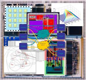
It is desirable to place the sensors and electronics on the same chip, and indeed there has been significant progress towards this objective in the last 3-4 years. Many problems remain unsolved, and the approach lacks the coherence of any methodology. Some key areas for research are:
- • Noise: always a problem, but if your signal is a single ion adsorbing on to a sensor membrane, then you will have your work cut out to measure it. Work is needed to understand and improve design techniques for such challenging applications.
- • We are familiar with foundry processes for IC and for MEMS devices, and it has been shown that electronic technologies can be combined with MEMS on the same chip, but where are the foundries that enable rapid prototyping of this sort? Similarly, there exist many tools for designing ICs or MEMS, but surprisingly little that combines the two. It is the lack of this resource that restrains the development of diverse microelectronic systems and merits research in its own right.
- • Sensors on microelectronics are possible, but often require occasionally exotic additional layers of processing. What is truly necessary, and what would be acceptable to mass manufacturers? Very little has been done.
- • Extremes of range: temperature; voltage; pressure; etc. There are, for example, high voltage processes that are widely available, but for the real extremes such as power electronics, and high tension (as might be used in an electro-osmotic pump for a microTAS) technologies are not presently compatible with low noise instrumentation design. Are there design solutions?
- • Methodology: large ICs used to be the unique preserve of specialised companies employing large design teams, but with the advent of system-on-chip even relatively small companies and design teams (usually working in the comms sector) can achieve remarkable results. Is there such a thing as a sensor-system-on-a-chip (SSOC)? Can we devise accessible design methodologies and tools to facilitate the proliferation of such devices?
The above is not complete, but should provide some pointers along a road we must follow in the next 5 – 10 years if the UK is to become a major force in new sector of global importance.