SpiNNaker Project - Boards and Machines.
SpiNNaker Circuit Boards
A number of PCBs have been produced to house SpiNNaker chips. These have been used to check the chips for correct operation and as platforms for software development. Most of the PCBs have a number of common features.- Power Supply. This takes a single DC input and provides regulated supplies of 1.2V and 1.8V for the SpiNNaker chips and other supplies (typically 3.3V) for other chips on the PCB. We have standardised on a 5V input for small (4 chip) PCBs and 12V for larger PCBs.
- LEDs. These are connected to SpiNNaker GPIO pins and are always useful for low-level software debugging.
- Ethernet Interface. This is the primary means of communicating with a SpiNNaker system from a host machine and is used for software loading and communication with programs running on SpiNNaker.
- SpiNNaker Link Connectors. These allow communication with the link ports on the SpiNNaker chips for debugging or to link multiple boards together to make larger systems. The connections are made with 34-way ribbon cable which is only suited to quite short connections. Links of up to 30cm are possible.
- JTAG Interface. Typically, all of the SpiNNaker chips have their JTAG ports connected in a chain. The chain visits every ARM968 core in a chip and this allows software debugging with a suitable JTAG adapter and debug software.
- Serial ROM. The on-chip bootstrap code in a SpiNNaker chip can load and execute code contained in an external serial ROM. This is used to load network parameters such as MAC and IP addresses but can also be used to load alternative code to that provided in the on-chip ROM.
- Clock Circuits. These provide a 10MHz primary clock for the SpiNNaker chips and also a 32KHz real-time clock (which is rarely used in practice).
- Test Facilities. Early PCBs contained numerous links and test points to aid with evaluation of the SpiNNaker silicon. For example, facilities for measuring current consumption. These have been phased out in later PCBs.
Spin1 (Test Chip) PCB
 The Test Chip PCB was the first to be produced and was used to
evaluate the first SpiNNaker chips. These chips had two major
differences to the current chips. Firstly, only two ARM968 cores were
present as opposed to 18 in the production chips. Secondly, although
the interface to a mobile DDR chip was present, the mobile DDR chip
was external. The production chips have the 1 Gbit mobile DDR housed
in the same package.
The Test Chip PCB was the first to be produced and was used to
evaluate the first SpiNNaker chips. These chips had two major
differences to the current chips. Firstly, only two ARM968 cores were
present as opposed to 18 in the production chips. Secondly, although
the interface to a mobile DDR chip was present, the mobile DDR chip
was external. The production chips have the 1 Gbit mobile DDR housed
in the same package.
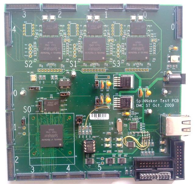
The PCB was designed and manufactured late in 2009 and was first used on 4 Dec 2009 when the test chips arrived from fabrication. The first PCBs had a BGA socket at the site at the bottom left of the PCB so that individual chips could be tested (as they were not production tested after fabrication). After a number of chips had been tested they were used to fully populate another batch of PCBs, one of which is pictured here.
The Ethernet connector is on the right hand edge of this board with the power input above it. The 12 miniature header plugs around the edges of the board are the SpiNNaker link connectors. The larger header plugs at bottom right are for JTAG and connections to the GPIO port on one SpiNNaker chip and for access to some Ethernet signals for debugging. The on-chip ROM on the SpiNNaker test chips was not fully functional and bootstrap code was loaded from the serial ROM.
The SpiNNaker chips are the 4 square chips (they are 300 ball BGA packages) and the 4 smaller rectangular chips are the 1 Gbit mobile DDR memories. A small number of patch wires were required to make this PCB fully functional! The board is 150mm square.
Spin2 (Production Chip Test) PCB
 The Spin2 PCB was designed to test the first batch of production chips
which arrived in May 2011. These have a different BGA footprint to the
test chips and so a new PCB was needed, although the overall design
is very similar and the size is identical. The production chips have
their mobile DDR memory inside the SpiNNaker package. The Spin2 PCB
has sites for external memories and these were fitted on early PCBs
just in case there was a problem with the in-package device. As the
internal memory turned out to be OK, later PCBs were made without the
external memory fitted, as seen here.
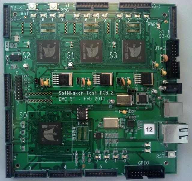
The Spin2 PCB was designed to test the first batch of production chips
which arrived in May 2011. These have a different BGA footprint to the
test chips and so a new PCB was needed, although the overall design
is very similar and the size is identical. The production chips have
their mobile DDR memory inside the SpiNNaker package. The Spin2 PCB
has sites for external memories and these were fitted on early PCBs
just in case there was a problem with the in-package device. As the
internal memory turned out to be OK, later PCBs were made without the
external memory fitted, as seen here.
Again, a couple of early PCBs were made with a BGA socket rather than soldering SpiNNaker chips to the PCBs. These were used (and still are!) for screening chips for functionality as we are not (yet) running post-production tests. This is only feasible for testing quite small numbers of chips and work is underway to develop post-production tests for volume chip production.
This PCB added a USB interface and an Atmel microcontroller to drive it while allows the board to be remotely reset rather than having to manually press the reset button. Some testing features were omitted from this PCB. Each SpiNNaker chip has 4 LEDs available on I/O pins (as did the test chip PCB).
The number of link connectors was reduced somewhat on this PCB and we also did an experiment to see if two links could be reliably sent down a single ribbon cable (they can't, due to cross-talk!).
Spin3 (General Purpose/Robot) PCB
 The Spin3 PCB was designed to fit inside a mobile robot. This meant
that it had to be physically smaller and also more power efficient
than the Spin2 PCB. It also houses 4 SpiNNaker chips but this time
on a PCB measuring 90 by 80mm. The power efficiency is improved by
using a switching DC-DC converter rather than the linear regulators
used in Spin1 and Spin2.
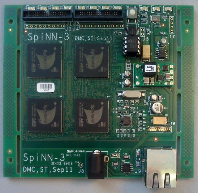
The Spin3 PCB was designed to fit inside a mobile robot. This meant
that it had to be physically smaller and also more power efficient
than the Spin2 PCB. It also houses 4 SpiNNaker chips but this time
on a PCB measuring 90 by 80mm. The power efficiency is improved by
using a switching DC-DC converter rather than the linear regulators
used in Spin1 and Spin2.
We realised during the design of this board that it could be quite easily extended to produce a general purpose PCB for software development and other applications. This just meant adding an Ethernet RJ45 connector, a power socket and a regulator chip. These live on the bottom section of the PCB as pictured here and can be cut off to create a board suitable to go in the robot. The strips to left and right of the board are tooling strips, used in PCB manufacture, and normally removed.
In keeping with its small size, this board omits some components from
the Spin1 and Spin2 designs. Each SpiNNaker has only 2 LEDs and only
two SpiNNaker links come to connectors. A minimal JTAG interface is
provided and 8 general purpose I/O lines from one of the SpiNNaker
chips. There is no provision for external DDR memory devices.
Spin4 (48 chip) PCB
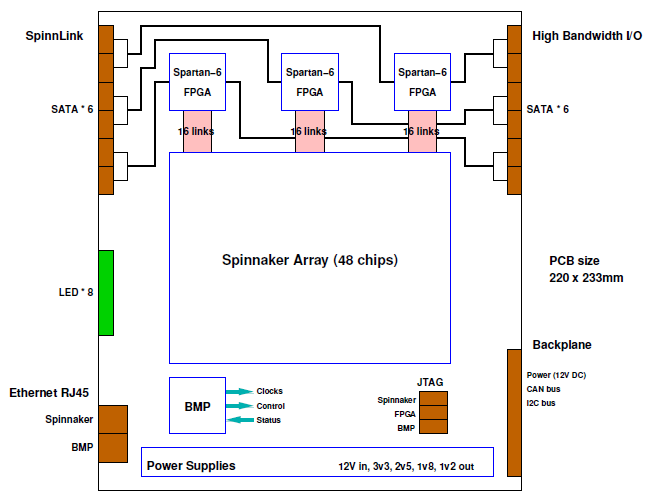 The Spin4 PCB is currently (Q1 2012) under development. It is the
first board which houses significant numbers of SpiNNaker chips. A
(logical) hexagonal arrangement of 48 chips is used and it is intended
that these boards will tile together to build very large SpiNNaker
systems. Rather than use lots of ribbon cables to connect boards
together, inter-board links are concentrated in FPGAs and converted to
serial format. The high-speed serial interfaces on the FPGAs drive
standard SATA hardware at 3 Gbps and SATA cables are used for
board-to-board connections.
The Spin4 PCB is currently (Q1 2012) under development. It is the
first board which houses significant numbers of SpiNNaker chips. A
(logical) hexagonal arrangement of 48 chips is used and it is intended
that these boards will tile together to build very large SpiNNaker
systems. Rather than use lots of ribbon cables to connect boards
together, inter-board links are concentrated in FPGAs and converted to
serial format. The high-speed serial interfaces on the FPGAs drive
standard SATA hardware at 3 Gbps and SATA cables are used for
board-to-board connections.
A standard Eurocard board size has been chosen (220 x 233mm) so that the boards can be housed in standard card frames. We estimate that the power consumption of the board will be around 75W (max) and so getting power onto and heat off the boards will be a significant issue.
Earlier PCBs used Ethernet (at 100Mbps) for all of their host and peripheral I/O and this has proved to be a bottleneck. Providing Ethernet connections to all 48 chips on Spin4 would be very difficult and so we are using spare serial interfaces on the FPGAs to provide a high-speed I/O facility. Of the 12 serial interfaces provided by the 3 FPGAs that are used, 6 provide network connectivity for SpiNNaker links (SpinnLink) and 6 are available for I/O. We propose to develop an I/O standard for SpiNNaker peripherals based on an in-house protocol running over SATA hardware.
SpiNNaker Load Board PCB
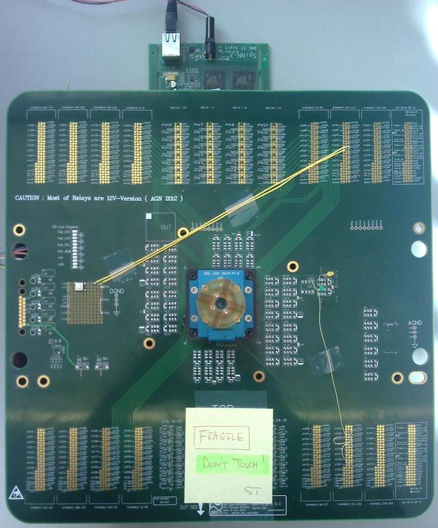 The SpiNNaker Load Board PCB is a special-purpose PCB which has been
developed for us by Smartest for
production testing of packaged SpiNNaker devices. The picture here
shows it being debugged (the temporary patch wires will be removed
before it goes into active service!). A Spin3 board can be seen in the
background which is being used to upload code onto this board via a
SpiNNaker link connector on the underside of the PCB.
The SpiNNaker Load Board PCB is a special-purpose PCB which has been
developed for us by Smartest for
production testing of packaged SpiNNaker devices. The picture here
shows it being debugged (the temporary patch wires will be removed
before it goes into active service!). A Spin3 board can be seen in the
background which is being used to upload code onto this board via a
SpiNNaker link connector on the underside of the PCB.
This PCB attaches to a chip test machine (a Teradyne J750 in our case) and a mechanical handler inserts SpiNNaker chips, one by one, into the socket at the centre of the board. Test patterns are then applied and the chip is then either passed as fit for use or rejected because a defect has been found. We are currently (Q1 2012) developing test programs for this board. A second load board is being developed which replaces the socket with a set of 300 probe wires which allow bare SpiNNaker die to be tested in a similar manner.